

This article deals with the possibilities open to an electronics' developer nowadays to optimise devices and circuits in terms of EMC. Due to much smaller circuit structures and lower supply voltages, the level of emission sources has dropped in the field of EMC emissions. This advantage, however, is cancelled out by higher signal frequencies as a result of increasing performance. Consequently, not much has really changed for emissions in general. Electric drives in vehicles are one exception here. Problems arising from RF currents which did not occur in applications without electric drives have greatly aggravated the situation.
There has been a general increase in EMC immunity problems. This is due to the ICs' lower supply voltages and shorter switching times.
The IC immunity levels drop with decreasing supply voltages. Due to their high speed, the ICs even identify short pulses as interferences.
Technological development in the field of electronics has brought about new EMC phenomena which require new specific EMC know-how. For example:
- ESD and ICs: modern, fast ICs respond to very short interference pulses in a specific way, thus leading to a completely new EMC behaviour in the devices under test.
- New technologies impose unprecedented technical demands: e.g. electric vehicles with respect to emissions
- New technical systems require high EMC standards for internal connections
Specialist know-how is an indispensable resource when it comes to breaking new technological ground. A consultant with expertise in corresponding special fields can provide just such know-how.
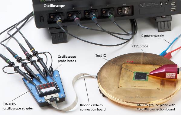
A consultant constantly has to come to terms with the latest, usually most complicated EMC problems. He can acquire the necessary know-how whilst solving these problems. The severest EMC cases from industry usually land on the consultant's desk. He needs to recall and apply his knowledge, but at the same time he is able to gain new experience. This work allows the consultant to recognise new EMC phenomena resulting from technical development as soon as they appear. This may even be years before these EMC phenomena are generally known in practice. Fast transients, for example, that occur during electro-static discharges can only affect fast ICs. New, as yet unidentified chains of actions are responsible for this phenomenon. The developer only sees the effect during an EMC test. The device under test reacts in an abnormal, inexplicable way (Figure 1).

The fast transients that occur during electro-static discharges last for approx. 200 ps. Only fast ICs can recognise them and can be affected by them. The duration of transient disturbances is so short that normal discharge systems are not able to short-circuit them. This means that the disturbance voltage is able to build up to its maximum and interfere with the electronics even though the specialist assumes that everything is perfectly short-circuited. The resulting fault patterns are abnormal and no longer allow an unambiguous interpretation
This effect is quite common today, but ten years ago it was rather rare. Once the problems that lead to this phenomenon are known, they can be controlled. The consultant learns fast while dealing with these and providing advice and is thus able to be of assistance in solving further problems expediently and efficiently.
The extent to which intervention in the development process is necessary depends on the respective EMC problem to be solved and may entail more or less work. The following global possibilities exist to suppress interference in devices:
- change the component packaging
- change the layout
- replace the IC which is responsible for the weak point
- improve the IC which is responsible for the weak point
- change the housing and/or mechanical design
To 1) Changing the component packaging is the easiest solution. It is what customers hope for, but this is generally to no avail since the problem usually sits deeper.
To 2) Layout changes mean that the printed circuit board has to be redeveloped. The movement of test points may affect the test adapters.
To 3) Replacing an IC with a QFP housing by an IC with a BGA housing may be successful but assumes that an IC with a BGA housing which provides the same functions is available.
To 4) If the volume of the entire project is large enough, it is also possible to improve the IC together with the IC manufacturer. This helps avoid a lot of additional design work in order to protect the IC from outside.
To 5) Design changes relating to the entire product require a lot of work. The simplest case would be a shielding part which can be added. Other cases may require the redesign of metal and plastic parts.
In general there are two different types of consultancy:
a) Consultancy in a crisis
A product launch is hindered by persisting EMC problems (Figure 3). Things begin to get desparate. The consultant is asked for help.

b) Consultancy during the development process
Consultancy during development usually arises out of the customer's experience. The idea springs from previous crisis consultancy when new projects are pending which involve EMC demands never experienced before. These may be new developments with a 10 to 100-fold higher performance factor that require the use of innovative technical principles for the first time. Such developments can break new ground and may even be new for the consultant too. One obvious approach would be to build and use prototypes to test all necessary measures. But experience teaches us that complex systems cannot be controlled in this way. There will be several weak points which usually overlap impenetrably in the prototype. A solution will be found in the end, but it will not be satisfactory. A lot of time and money will finally lead to a lame compromise.
Splitting the total system into individual parts, however, has proved its worth. Based on the cause and effect relationship, the device has to be broken down into elements. This will be demonstrated here taking a high-speed bus system as an example. The bus system has to work correctly in all circumstances, even if an electro-static discharge causes a bit error. The signal path of the high-speed bus system has to be divided into individual components such as: transmitting – receiving IC, printed circuit-board segments, connectors and cables. All of the components are tested separately for their suitability and improved as necessary. Corresponding EMC objectives have to be defined for this purpose. Last but not least, the optimised components are assembled in an initial sample. This will be immune to interference if the consultants and their customers have worked together properly.
The high-speed connector component will also be examined here. Setting up a test system in the form of a high-speed section (prototype of the high-speed system) would not be flexible enough. It is much better to know the connector's physical parameter that represents its function in interaction with the ESD disturbance path, namely the coupling inductance. This parameter describes the relationship between the ESD disturbance current flowing on the plug pin's outer sheath and the voltage induced on the inner signal lines. The coupling inductance is a frequency-independent constant which only depends on the connector's design. This means that each connector has its own individual value. When the maximum ESD disturbance pulse flows across the plug connector from outside, the voltage in the signal lines may not exceed the high-speed IC's immunity level. If the induced voltage is greater, the ESD disturbance will interfere with the high-speed system. The following worst case scenario can be designed for practical purposes: the connector should be able to carry the total 6 kV ESD disturbance current of IESD = 22.5 A (current according to EN 61000-4-2). The high-speed receiver has an immunity level US of approximately 100 mV.
The required coupling inductance can be calculated from
L = 3 pH.
3 pH is a very small value for a plug connector. Plug connectors usually have coupling inductances between 30 pH and 1,000 pH. There is hardly any connector that can solve this problem. The situation can be remedied with an additional shielding plate over the connector. Such solutions cost time and money.
The connector manufacturer is not usually aware of how important the coupling inductance is. That's why connectors which may possibly fit the purpose have to be bought and measured to find a suitable one. If the project is large enough, a bespoke connector may have to be developed especially for this application. This would be the most elegant approach. Of course, the plug connector manufacturer can develop a connector relatively quickly according to the coupling inductance requirements. A coupling inductance measurement set-up (Figure 4) and a simulation tool will help him.
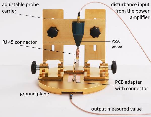
If, for example, a metal part is bent or moved slightly at the coupling inductance measurement set-up, the effect on the inductance can be seen immediately at the measuring device. This procedure allows a quick optimisation of the connector. The target value for the connector should be a coupling inductance of approximately 1 to 2 pH, which is an inconceivably small value for a plug connector. Once the target has been achieved and the finished connector is inserted into the initial sample, the connector system will pass the ESD test.
All EMC-relevant components which are located on the disturbance path of the high-speed system have to be treated in the same way.
The initial sample will fail if this approach is not taken and a conventional connector whose coupling inductance is not even known is used instead. In this case the decision about the design will have been taken and in most cases the production tools will already have been built. It will be difficult or even impossible to find a second suitable and compatible connector. At this point, there are two possibilities: to design an additional shielding part over the connector or to redesign the entire device.
It is a consultant's task to make sure that the right approach is taken from the very outset together with the electronics' developer. The examples also clearly show the benefits of consultancy during the development phase compared to crisis consultancy.