

The number of mobile devices such as smart phones, tablets and wearables has risen significantly over the past years. At the same time, wireless communication has increased due to higher data rates. Will the growing number of wireless devices multiply the EMC problems? Is today's industry able to cope with the EMC requirements that the Internet of Things has in store for us?
If more devices have to interact with each other and their EMC quality remains at the present level, this will lead to more EMC problems from a statistical point of view. Furthermore, a device may be incompatible in practice even though it has passed the compliance test. Let us assume that an electronic device has passed the emission compliance test according to IEC 61000-6-3, IEC 61000-6-4, for example. In contrast to the test, the electronic device may be located near a metallic object such as a housing in practice. This may lead to field coupling which in turn results in higher emissions than in the test. The dimensions of the metallic object are essential in this context. The field may stimulate standing waves that fit the dimensions of the metallic object and then cause additional emissions.
This means that in future, not only will wireless transmission problems arise but also problems due to emissions from devices.
Stricter device standards will not necessarily solve this compatibility issue.
The example above shows that the current compliance tests usually do not take any field coupling mechanisms into consideration. The field coupling mechanisms may induce some helpful ideas on how to solve the problem.
It remains to be seen whether the measuring principles specified by the current standards are sufficient or whether new measuring principles will have to be developed.
Furthermore, new requirements are emerging in the field of EMC standards for ICs (IEC 61967 and IEC 62132). Concrete IC EMC parameters will be needed as input values for EMC development tools / simulation programs for PCBs in future. It would be sensible to obtain these EMC parameters from measurements according to IC EMC standards. Unfortunately, the results of standard measurements are currently inadequate for such a purpose.
This procedure will become more important for IC development in the future.
These are the reasons why one should consider adapting the test methods of the standard measurement to this task. This will be shown below for ICs by taking conducted emissions as an example.
The interference suppression strategies currently used in electronics development come up against their limits. ICs as potential emission sources are not noticed as troublemakers until the first development sample has been completed. The developer comes across them when taking interference suppression measures in the device or on the PCB. Near-field probes are used to locate RF sources in the electronics. These do not identify the IC itself as the disturbance source but PCB traces into which the IC feeds disturbance currents and disturbance voltages. The electronics will then be modified with additional components, copper foil or other means. Last but not least, EMC measurements are carried out to confirm the success of the interference suppression measures taken after the redesign of the PCB.
This approach is very time-consuming and expensive. One big problem here is that selective EMC measures cannot be taken until the first functional development sample has been completed. Insights which could be crucial for EMC are gained when it is too late. Important decisions are taken in the development process without considering the results of the EMC test. Problems are almost inevitable because the EMC test results are obtained at such a relatively late point in time.
However, the industry demands faster and more efficient developments in compliance with EMC. This can only be achieved by taking a completely new approach. This has to begin early on in the development process and delves deep into the emissions' chains of action. Only hands-on knowledge of the emission source allows the developer to follow this path. Once ICs have been described more precisely as potential sources of emissions, appropriate measures can be taken much earlier and more efficiently to stabilize the whole device's EMC.
Appropriate EMC parameters are a prerequisite and are thus subject to high demands. They have to describe the EMC problem zones of the ICs for practical use in industry. This means they must be suitable for the development of PCBs in compliance with EMC requirements. In addition, the IC's EMC parameters must be linked with practical measures and strategies.
This approach should define electronics development in terms of EMC. On account of extreme miniaturisation, a higher susceptibility to electromagnetic disturbances is experienced in the field of device development today. The device manufacturers make increasing efforts to address the problems so as to suppress interference in devices and comply with the corresponding standards.
The problems described in the example above aggravate the situation even more. An important requirement for the Internet of Things in particular is that the devices function properly and reliably in their environment.
The extent to which device manufacturers can continue to master the EMC situation which is aggravated on account of the miniaturisation and to suppress interference in devices by spending more time and money on this work remains to be seen. Development in compliance with EMC requirements will represent an increasing share of the costs in device development. It is doubtful whether the EMC objectives will be able to be fulfilled at all. This problem can be mitigated by providing better EMC parameters in the fields of IC research and IC development in future. However, this means that more time and money will have to be spent here too. Of course, this relates to the wireless devices. German industry has started to respond to this mounting pressure.
Companies now work together with EMC advisors in solving EMC-related problems in the development of devices and complex systems by using new EMC technologies from the very beginning of the development process.
Main part
Due to internal functional operations, ICs generate RF voltages, currents and fields. Different physical mechanisms are responsible for these entering cable harnesses in the form of emissions or the surrounding open space in the form of radiation. ICs may have the following effects:
- Conductive: emission of RF currents and voltages via the IC pins into the PCB traces,
- Capacitive/inductive: emission of E- and H-near fields from the die or connections of the IC,
- Radiative: direct emission of electromagnetic waves. Direct emissions are usually only crucial in the Gigahertz range for ICs with very high clock rates in practice.
The following section describes Item 1 and 2: conductive, capacitive and inductive effects in the PCB.
Emissions follow a closed loop. The driving RF-current and RF-voltage sources are located inside the IC. They drive RF into the PCB traces via the bonding wire, lead frame and pin where the current generates magnetic near fields and the voltage generates electric near fields. The electric and magnetic near fields would build up undisturbed if a PCB trace were to be freely positioned in space. The fields are similar to the E-fields and H-fields of an antenna. The electric field is closely coupled to the magnetic field via the antenna element, its current and voltage. This electric field pattern results in the emission of electromagnetic waves. The PCB trace acts as a transmission antenna.
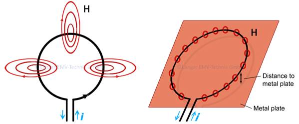
The situation, however, is usually quite different on the PCB. The PCB contains metal surfaces. These metal surfaces usually extend over the entire PCB and have ground or supply voltage potential. The gap between these metal surfaces and the PCB traces is normally < 1 mm. These ground surfaces affect the distribution of the trace's electromagnetic field. The effect can best be described by taking a loop antenna as an example. A loop antenna can emit electromagnetic radiation if positioned freely in space. If the loop antenna is placed on a ground surface, this will prevent the emission of electromagnetic radiation. This is because the corresponding conductive metal surfaces block the magnetic field in the opening of the loop an account of current / field displacement effects (skin effect). The loop antenna's magnetic field can no longer build up around the antenna and is practically no longer present. Radiated emissions from the loop antenna are thus reduced considerably (Figure 2).
The PCB trace reacts in precisely the same way. Direct emissions from the trace are prevented as soon as the ground surfaces in the PCB are large enough. Emissions from the trace will not increase until this is at a certain distance from the ground surface. The required distance depends on the length of the trace. Practical experience shows that the gap must be > 0.5 cm to cause any effective emissions (frequency range < 1 GHz) with a trace length of > 10 cm.
This means that emissions take other ways from a PCB, namely via its near fields.
These near fields cause emissions through interaction with metal parts (Vdd/Vss surfaces, large metal components, cables and lines, metallic structural parts).
Relationship between IC voltage and emissions
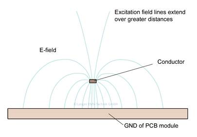
We refer to the PCB trace in the following text. The traces inside the IC follow the same principles. The statements on the PCB trace can thus be transferred to the traces inside the IC. The pin voltage which is present on the PCB trace or the trace inside the IC builds up an electric field around this trace (Figure 1). Most of the field lines lead to the PCB's GND surface. Only a few field lines leave the PCB vertically upwards and penetrate into open space. The closer the trace is to the edge of the GND system, the more field lines penetrate the space.
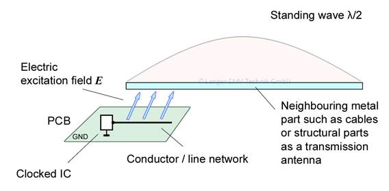
These field lines (excitation field lines) leave the PCB's GND system and carry displacement current through space which stimulates the entire metal system (PCB with cables and metallic structural parts) to vibrate electrically (Figure 3).
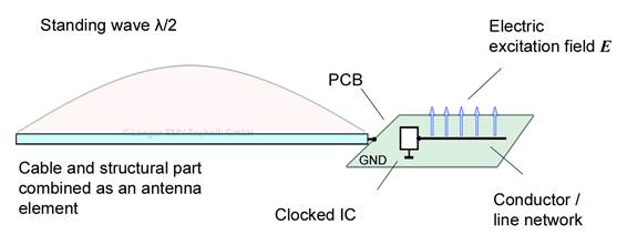
The standing waves on the metal system may cause emissions.
The electric excitation field may reach metal parts (cables, structural parts, shielding plates, Figure 4) located opposite the PCB and these may be stimulated to vibrate electrically by the transferred displacement current.
Relationship between IC current and emissions
The IC's current loops can either be located inside on the die or loops can be formed by the IC's pins. These loops run through the ground system of the PCB, pin, lead frame, bonding wire and die. This type of loops can be formed via Vdd or Vss pins, for example. The Vdd / Vss loops that penetrate to the outside may be much larger than the loops located inside the die. The larger outer loops can generate a stronger magnetic field and are usually responsible for the highest emissions.
We refer to the PCB trace in the following text. The traces inside the IC follow the same principles.
The statements on the PCB trace can thus be transferred to the traces inside the IC.
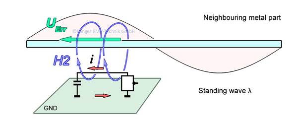
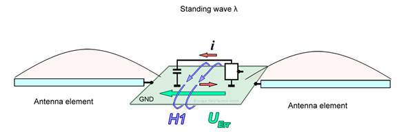
The pin current which flows into the PCB trace builds up a magnetic field H2 (Figure 5). The returning pin current also generates a magnetic field H1 in the GND system (Figure 6). It is assumed that the PCB ground is a metal surface which extends over the entire PCB. The trace is so close to the ground that it can usually only generate insignificant emissions, as in the loop antenna example above. The field H1 of the returning current induces a self-induction voltage UErr. in the GND plane of the PCB (metal surface). This voltage drives cables and structural parts that are connected to it like an antenna. The cables and structural parts emit electromagnetic waves as a result.
The magnetic field H2 (Figure 5) of the trace cannot generate any radiated emissions in open space. This is due to the fact that the trace is close to the ground plane, similar to the loop antenna example above, thus preventing emissions. There is another chain of interactions that causes the magnetic field to radiate emissions. This is similar to the one described for the field H1 above. A metal part has to be inserted into the field H2 for this purpose. An excitation voltage is only induced there via mutual induction if the magnetic field encloses a metal part. The excitation voltage stimulates the metal part to act as an antenna. The metal part emits electromagnetic waves. A steering column, a metal strut or a cable in the PCB's neighborhood in a vehicle is taken as an example.
EMC parameters for IC pins
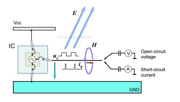
The IC pin current and IC pin voltage are the pin-related EMC parameters of an IC. The IC's electric near field and magnetic near field are the field-related EMC parameters of an IC. All four parameters (u, i, E, H) of the IC have to be detected by suitable measuring devices.
The electric near field of the PCB traces is proportional to the pin voltage and the magnetic near field of the conductor loops of the PCB is proportional to the pin current of the IC. The pin current and pin voltage depend on the load to which the pin is subjected through the connected PCB trace.
The values of the cases in which the highest pin voltage and the highest pin current are generated have to be used for the IC parameters.
The current and voltage of the traces depend on the driving voltage in the IC and on the impedance of the load on the PCB traces.
The maximum possible pin current is measured if the pin is operated under short-circuit conditions. The maximum possible pin voltage is measured if the pin is operated under no-load conditions (open circuit). The maximum possible values have therefore been determined and all values from practical operation (determined in a large number of measurements on different PCBs) are equal or smaller.
The voltage, and thus the electric near field, are highest under open-circuit conditions in the PCB traces in special cases. The emission potential is then at its greatest.
The corresponding EMC parameter of the IC is its open-circuit voltage Ul(f).
The magnetic near field is proportional to the current flowing through the trace. The current depends on the IC's driving voltage and the load of the trace. A short circuit may occur in special cases. The current, the magnetic field and thus the emissions are then at their greatest.
The corresponding EMC parameter of the IC is its short-circuit current Ik(f).
The maximum pin current and pin voltage values (Ul(f), Ik(f)) are produced under short-circuit or open-circuit pin conditions. In these cases, the highest emissions are generated via the coupling mechanisms described above.
Hence, it follows that each pin of an IC has its own EMC parameters for conducted emissions. An IC pin's EMC parameters are its open-circuit voltage and its short-circuit current.
The open-circuit voltages and short-circuit currents can be determined for most pins of the IC through measurements under close to open-circuit and short-circuit conditions. Two spectra for each pin result in 128 spectra for a 64-pin IC, for example. Furthermore, the pin can have different switching states (input, output H, L and high-impedance). The internal function may also assume different states (Clk-PLL OFF/ON).
The current in the power supply pins is measured according to the 1 Ohm method. If the resistance of 1 Ohm is too great, a 0.1 Ohm measuring resistor is used. This measurement can be carried out in both the Vdd and Vss. A corresponding high-impedance probe and a decoupling capacitor can be used to measure the RF open-circuit voltage on crystal oscillator pins. The crystal oscillator's filter capacitor may serve as a decoupling capacitor.
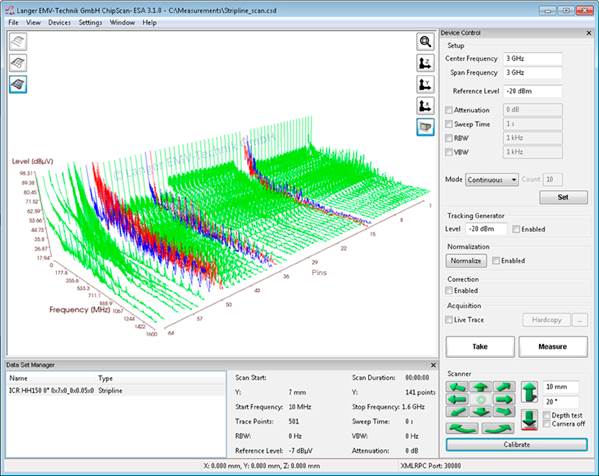
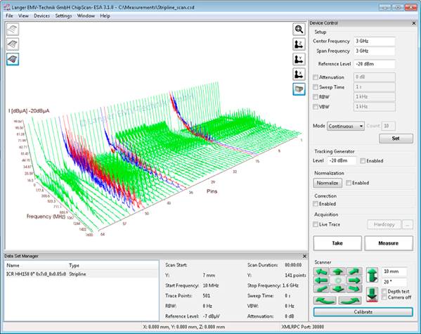
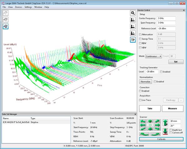
The measurements may produce a large amount of data and become difficult to manage. A 3D representation provides a clear overview of the results (Figure 8). A custom-developed measurement set-up with a corresponding software (ChipScan ESA) allows a semi-automatic recording of the pin spectra. The results are visualised in 3D. The representation can be switched over to 2D for selected pins (Figure 12).
Use of IC parameters
The 3D spectra clearly reveal the problematic pins for practical applications. Open-circuit voltages in the range of 80 dBµV can lead to limit-exceeding emissions over trace lengths as short as approx. 10 mm (particularly problematic in automobiles). The critical frequency range can be read from the 3D – 2D spectrum. Figure 12 shows this for the crystal oscillator pin 15. The critical frequency range extends up to 600 MHz. The layout and design can be steered in the right direction on the basis of the EMC parameters of the IC pins to save time and money. There will be ICs where individual pins display high values in terms of conducted EMC parameters of the emissions. These values provide helpful advice on how to use the IC on the PCB in a compatible way. Consequently, these ICs need not be excluded from developments. IC users should determine the IC's EMC parameters before they start developing a PCB.
If ICs are integrated without this information (as it is still common practice today), problems will not arise until the first development sample has been measured. This entails high costs for time-consuming interference suppression measures (layout changes, design modifications, etc.). This approach also permits an IC to be chosen from a range of alternatives because it will most likely cause lower emissions, and hence it will be easier and less costly to make its PCB assembly EMC compliant.
Two new helpful tools can be created for electronics development on the basis of the IC's EMC parameters:
- Pin-related open-circuit voltage and short-circuit current spectra (3D / 2D)
- Layout and design tips in conjunction with the EMC parameters of the IC pins
An EMC specialist can derive such design tips (counter-measures) from the pin spectra, interactions (items 1 and 2) and the character of the special application. However, design hints and tips should better be provided in the form of pin information in practice. The EMC parameters Ul(f), Ik(f) of the IC pins can be grouped in frequency-dependent level ranges with different risk potentials. A certain barrier of design measures has to be built up depending on the risk potential. This strategy will be the basis of EMC activities over the years to come.
Examples of pin-selective counter-measures in terms of open-circuit voltage:
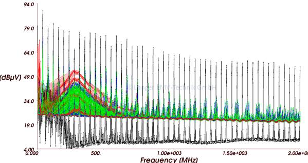
The static port pins 16 to 35 Figure 8 show high open-circuit voltages. This leads to emissions via the electric field if several port conductors are connected to PCB traces. As a counter-measure, the traces should be well enclosed by GND and not be located at the edge of the PCB.
Examples of pin-selective counter-measures in terms of short-circuit current
The port pins 16 to 35 also provide relatively high short-circuit values (Figure 9). Filter capacitors located further away can generate critical current loops. As a counter-measure, the filter capacitors should be located in the vicinity of the IC or series resistors should be inserted.
High values are obtained for the supply pins 12, 13 in the lower frequency range (< 100 MHz) and pins 50, 51, 52 in the medium frequency range (around 500 MHz). As a counter-measure, the current loop that passes over the blocking capacitor can be attenuated with a resistor (< 10 Ohm) or a soft ferrite. The blocking capacitors and the IC should not be too close to the edge of the PCB (> 20 mm). The IC should be positioned so that the IC current loop is orthogonal to the PCB's longest axis. This holds particularly true for PCBs that are not wider than 50 mm. The orientation of the IC current loops can be measured with field probes designed for RF field measurements on ICs and provided as IC EMC field parameters.
Measurement systems for EMC parameters of IC pins
Figure 10 shows the measurement set-up for pin current and pin voltage measurements.
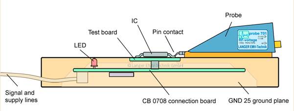
The test IC (DUT) is placed on a test board which is embedded in a ground plane. This provides a continuous GND surface as a prerequisite for measurements up to the GHz range.
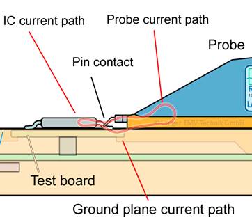
A (voltage or current) measuring probe whose tip can be moved easily to contact each pin is placed on the GND plane. The measuring path (IC - pin contact - probe) is only a few millimetres long so that the measurement can be carried out at a short electrical distance. The IC is supplied and controlled by the connection board via filters (Figure 10). The connection board is integrated into the ground plane
Practical example
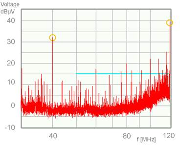
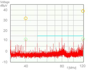
Figure 11 summarises the results of a measurement on vehicle components. The limit value violation of 24 dB occurs at 120 MHz due to an E-field. This problem was not discovered until the development sample was tested. A measurement of the open-circuit voltage Ul(f) of the IC pin as one of the IC EMC parameters reveals the cause.
Exceptionally high voltages (approx. 80 dBµV at 120 MHz) were measured on the IC pins for the crystal oscillator in a 40 MHz grid (shown in black in Figure 12).
All lines and metal parts connected to these pins emit an electric field as described under Item 1 of the physical mechanisms. The electric field is exceptionally strong and causes the PCB and the cable harness to vibrate electrically.
This means that the field is coupled out via:
- the bonding wires and lead frame of the IC pins that lead to the crystal oscillator,
- the 15 mm PCB traces from the IC to the crystal oscillator,
- the crystal oscillator housing and crystal oscillator wiring 3 x 0603 SMD components.
A suitable remedy in this case is to reduce the surface of these metal parts, i.e. to shorten the traces and embed them in GND, to use smaller crystal oscillator housings. However, these counter-measures are not sufficient in our example. The open-circuit voltage Ul (f) of the pin is so high that the metal surface of the bond wire and lead frame is large enough to cause a limit value violation during the component measurement. Filter capacitors cannot be used to reduce the voltage on the crystal oscillator. An E-field shielding directly above the IC can be used as a final remedy. Figure 13 shows the positive results achieved thanks to these counter-measures. The limit values are met.
The EMC characteristics of ICs can already be determined today. It is useful if values obtained are entered in product data sheets. This information allows the developer to already plan EMC measures that are necessary for the PCB during the development process, so that in principle they can use any IC.
Test methods to determine the IC EMC parameters enable the IC manufacturer to develop ICs more efficiently.
Due to the continued miniaturisation of modules and the high number of very complex electronic devices, the EMC assessment of ICs is a valuable prerequisite for the future development of electronic devices.
The use of IC EMC parameters will also have a positive effect on the development of the Internet of Things.
Article is also published on the website of interferenctechnology