

IC EMC Parameters - Mechanisms of Interference Emission
Introduction
The interference emission behavior of an IC and the associated emission of a PCB assembly are difficult for board developers or EMC engineers to predict. If EMC weaknesses in and around ICs are detected too late, they can lead to extensive and costly redesigns.
More and more IC manufacturers are therefore checking whether the measurement results from new IC tests provide added value for IC users and contribute to higher customer satisfaction. In this process, IC parameters are defined that make it easier to use an IC in electronic applications despite high complexity. In automotive assemblies in particular, the IC is often the main source of emissions.
This article presents IC parameters and their measurement-based determination.
IC Near Fields
Due to their internal switching operations, integrated circuits generate electric and magnetic near fields. These fields are caused by currents and voltages inside the IC. The complex networks of an IC generate a large number of such fields.
The largest surfaces for E-field emission and the largest current loops for the induced excitation voltage are located in the pin, lead frame, and bond wire areas. It should be noted that pins with static or quasi-static signals can carry RF due to internal parasitic coupling.
RF voltages against GND can occur on internal metal parts of an IC. These voltages generate electric fields between the metal part and the GND system of the PCB assembly.
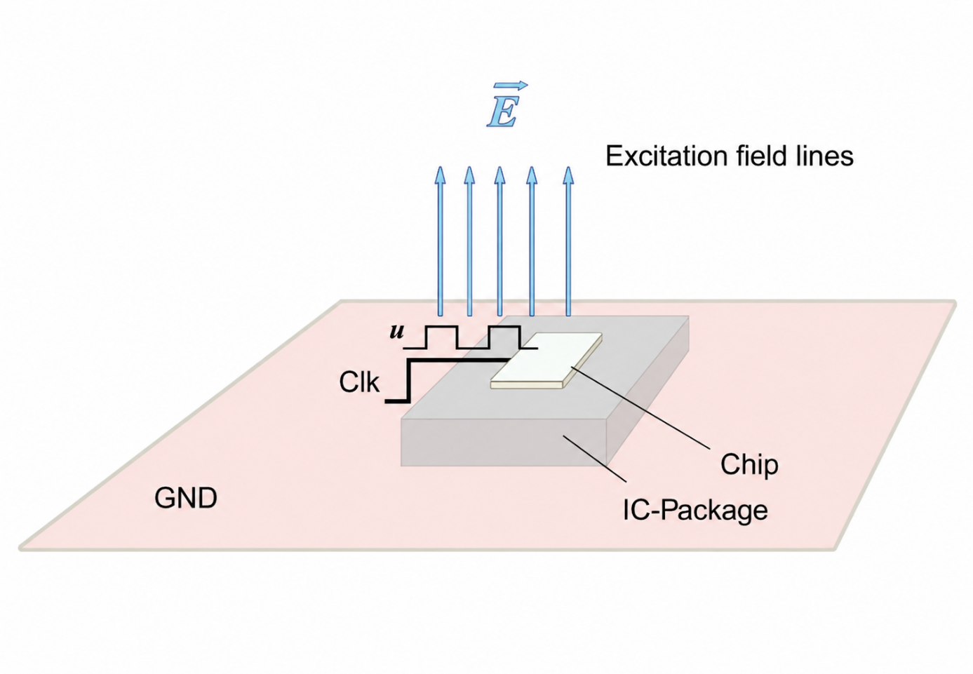
Most field lines reach the GND system over a short distance. A few exit vertically upward and extend far into the surrounding space (Figure 1). These field lines are the excitation field lines relevant for EMC analysis. They generate a displacement current. The resulting charging current can couple to nearby metal parts and excite the metal system as an antenna. Such nearby metal parts can include, for example, a cable harness, a steering column, a DIN rail, and many others.
Magnetic fields generated in current loops close to GND, such as Vdd-Vss loops, are divided into two components, H1 and H2, as shown in Figure 2.
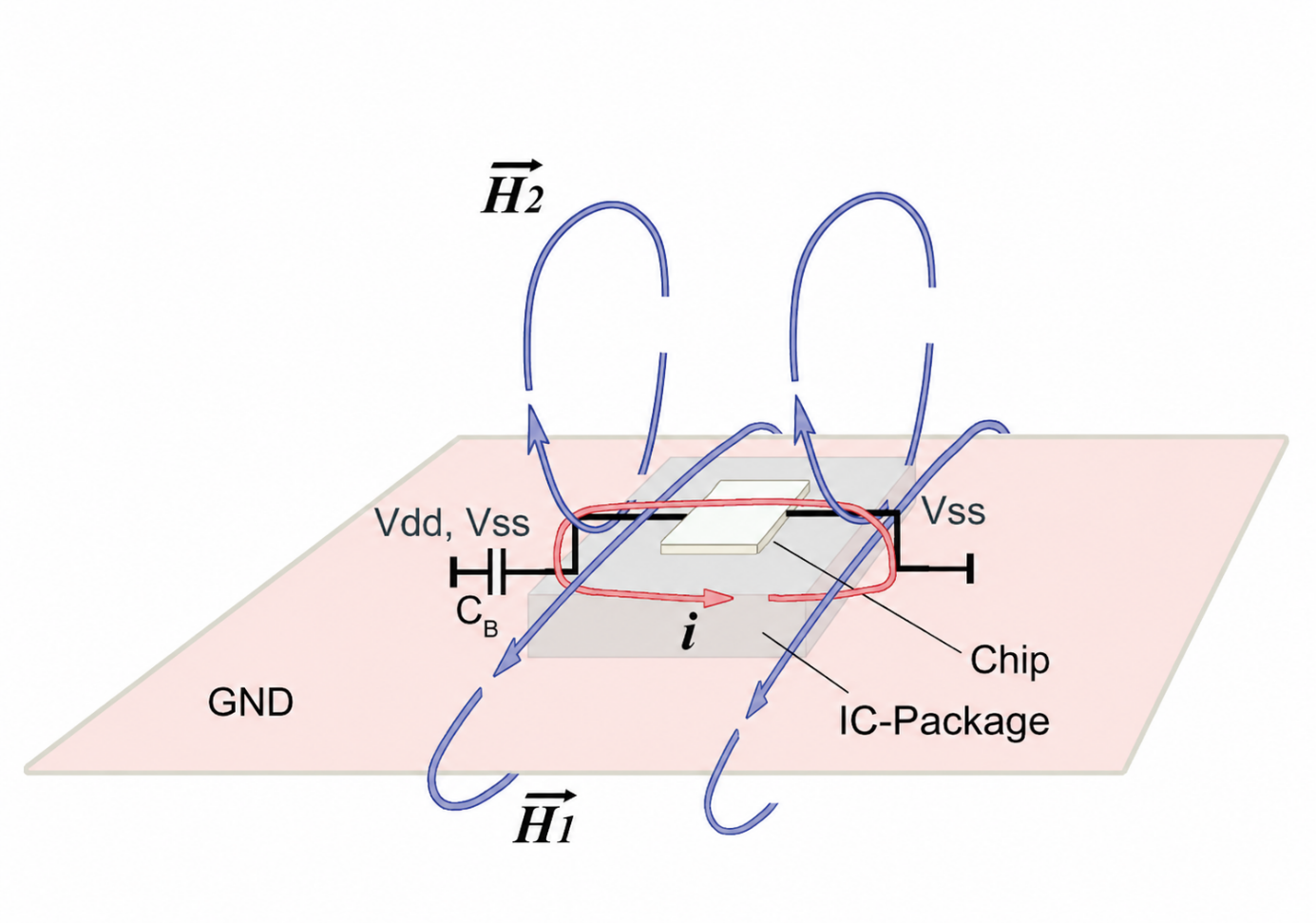
The H2 field forms at the IC-internal current conductor and closes in the space above an IC. The H2 magnetic field is the significantly stronger magnetic near field. Its effective range is approx. 10 cm. The surrounding area further away provides the transition to the far field in the meter range. If the H2 field encloses a metallic conductor, an RF voltage is induced in it. This voltage can excite the conductor and cause interference emission. These conductors can be the same metal parts as described for the E-field coupling above.
The H1 magnetic field is the weaker magnetic field. However, it encloses the metal plane of the PCB assembly and is therefore the most important for EMC analysis. Knowledge of the strength and direction of an IC’s magnetic field forms the basis for developing an EMC-compliant design of electronic PCB assemblies.
The E-/H-field-related coupling as well as the conducted current and voltage coupling are IC-specific quantities and can be measured in advance as parameters. If these parameters are known, the IC user can already plan EMC measures during the project planning phase
Measurement of IC Near-Field Coupling
The networks in an IC are so complex that a complete description of all currents, voltages, and electric and magnetic field couplings is hardly possible in practical applications. For measurement-based evaluation, it is therefore useful to focus on the essential parameters.
For emission, the conducted high-frequency currents and voltages as well as the magnetic and electric field flux are of interest.
Current and Voltage Measurement at the Pins (IEC 61967-4)
A two-terminal network is characterized by its open-circuit voltage and short-circuit current. Maximum interference emission is caused either by maximum voltage, which generates a maximum E-field, or by maximum current, which generates a maximum H-field. An RF open-circuit voltage measurement and an RF short-circuit current measurement are therefore useful for the physical characterization of an IC.
High demands are placed on the RF current meter, especially when selecting the shunt resistor. A 1 Ω shunt is sufficient for certain applications. However, for supply voltages below 5 V, a 0.1 Ω shunt may be more suitable.
Another parameter of an RF current meter is its internal inductance and its ratio to the loop inductance of the circuit. If several supply pins in an IC are internally connected at RF level and one of these pins is contacted with a current meter with excessive inductance, the RF current may shift to other pins due to the increase in impedance and distort the measurement. Therefore, the entire measurement setup must have extremely low inductance. Assuming an example loop inductance of 10 nH for an IC, the internal inductance of the current meter must not exceed 1 nH.
The design of the measurement device also determines the behavior during current measurement. Measurements on standing current or voltage waves must be avoided. From the frequency range for the measurement bandwidth of 10 kHz to 3 GHz, a wavelength of approx. 10 cm can be derived at 3 GHz. The measurement path and the IC share a correspondingly shorter length, so the measurement path may have to be realized in a very compact setup.
The emission mechanism via E-field and H-field excitation of nearby metal parts is effective only at distances smaller than λ/2. If no metal is present within this distance from the IC, the physical effect of direct emission dominates.
Near-Field Measurement above the IC (IEC TS 61967-3)
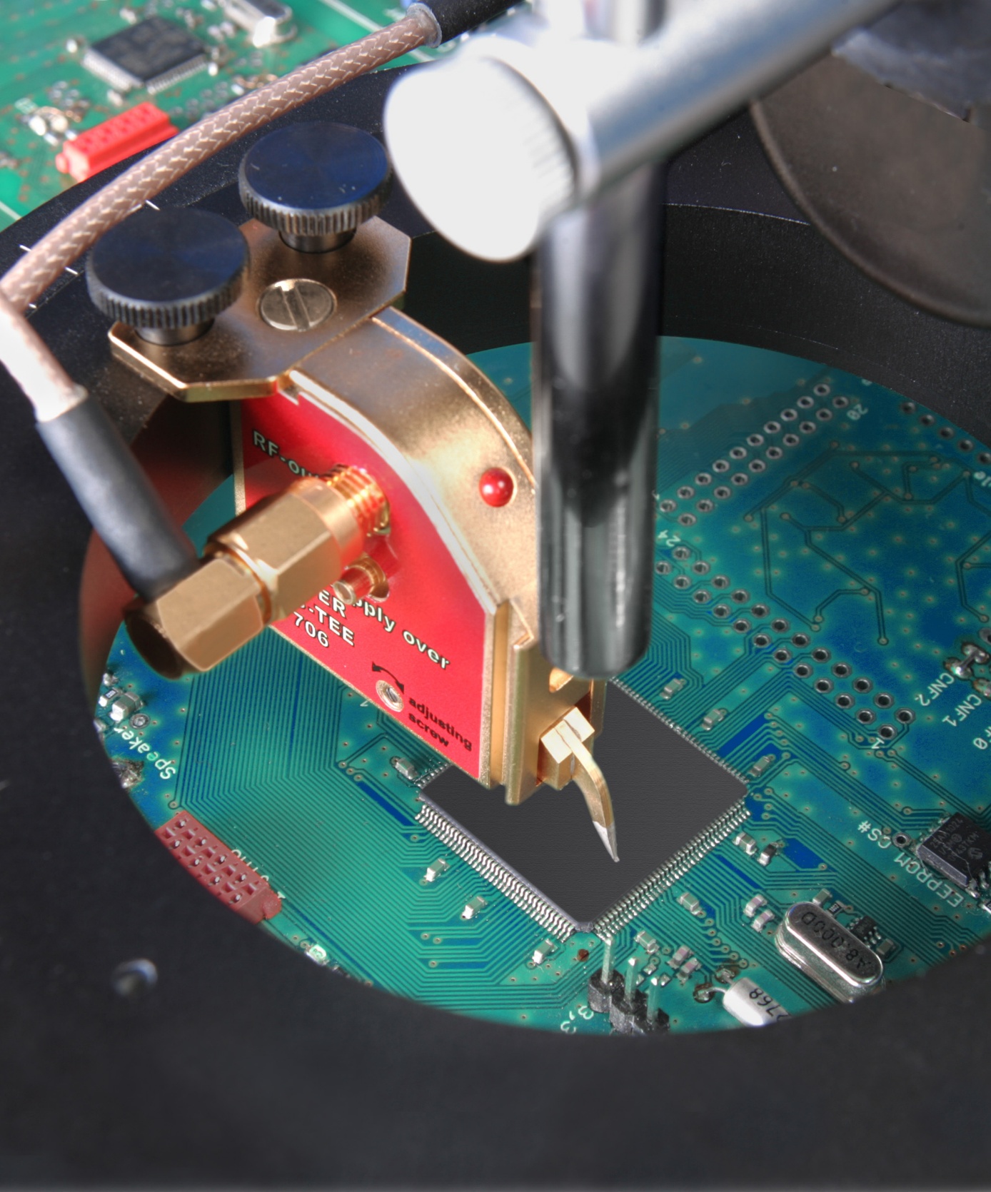
Measuring the spatial amplitude-frequency characteristic of electromagnetic emissions requires an IC test system architecture that includes the following components: in addition to a spectrum analyzer, near-field microprobes, a positioning system, and software for controlling the entire measurement sequence in the IC test system and for data evaluation are required.
To fully capture the EMC emissions of ICs, three types of near-field probes and an at least four-axis positioning system for the microprobes are required.
An E-field probe is needed to measure the electric field, and two H-field probes are needed to measure the magnetic field. The two magnetic field probes differ in their polarization plane: one H-field probe has horizontal polarization and one has vertical polarization. With this set, all field components of the EMC emissions above the IC can be captured.
The positioning system places the microprobes and determines the spatial coordinates of the electromagnetic field. Due to physical reasons, the vertically polarized H-field probe has two nulls in its directional characteristic. The field components located in the plane of the vertical probe are captured only by rotating the vertical field probe. Therefore, at least a four-axis IC Test System with x-, y-, z-, and a rotational axis is used as the positioning system.
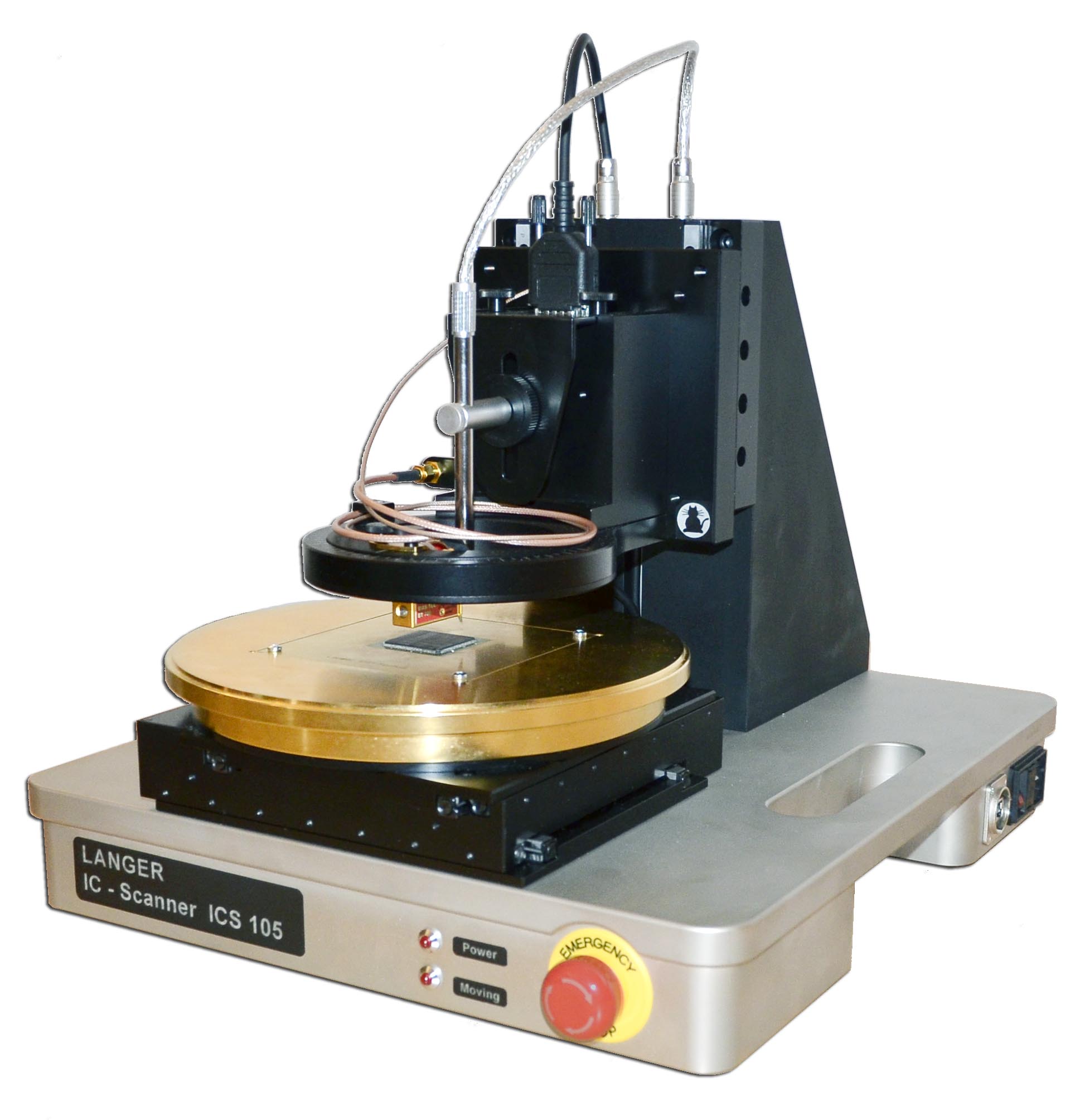
Figure 4 shows a basic arrangement of the IC test system for measurement using the Surface Scan method according to IEC 61967. The near-field microprobes are active probes with dimensions in the range of 0.1 mm to 0.5 mm. Due to their design, they allow separate analysis of electric and magnetic emissions at IC and die surfaces, bond wires, and pins.
The resolution and sensitivity of the probes require a precise positioning system that moves the probes point by point within the measurement volume. The actual E-field and H-field probe is arranged as a probe head at the probe tip. The complete probe is an active probe. The application range of IEC 61967-1 from 150 kHz to 1 GHz is fully covered and exceeded by these probes.
The IC test system of Langer EMV-Technik GmbH can accommodate all types of microprobes and larger near-field probes. These are moved point by point within the measurement volume by the four-axis ICS 105 positioning system. The position of the probe tip is checked using a digital microscope. The smallest step size of the positioning system is 10 µm. However, the measurement resolution of the near-field probes determines the useful step size for the complete IC measurement.
Volume Scan above the IC
Figure 5 shows the measurement result of a volume scan above the IC, recorded with the ChipScan software from Langer EMV-Technik GmbH.
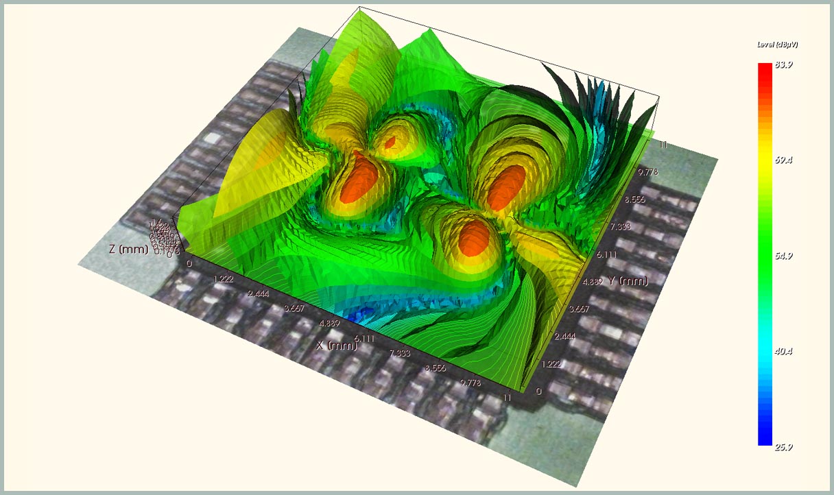
In this case, the measurement volume is 11 x 11 x 1.6 mm above an IC with 44 pins. The field sources can be located very clearly and easily. The field distribution on the surface allows conclusions to be drawn about the internal IC structure. In the spatial representation of the magnetic field, points of equal field strength are connected by ISO surfaces and shown in color according to their intensity (red: intensive interference radiation).
At the end of the measurement, surface scans are available for all frequencies of the measurement interval: one complete surface scan for each frequency point and each volume plane. By selecting the peaks in the measured cumulative spectrum and setting the corresponding frequency in the evaluation software, the field sources of the interference emissions can be located using the frequency value of the surface scan. Conclusions about the installation environment of the IC can be easily identified.
Using spectrum analyzers and near-field probes, preliminary investigations at PCB level are possible. In combination with an IC Test System, the development engineer can precisely locate EMC emissions and reproduce and document the measurement results.
In addition, different modifications for reducing EMC emissions can be compared. The spatial amplitude-frequency characteristic of the electric and magnetic fields is suitable for this, especially when a specific IC package type had to be used due to special layout requirements. By carrying out step-by-step IC tests during the development process, EMC conformity testing can be performed in a timely and cost-effective manner without unexpected issues.
Example Measurements on the IC
For a PCB assembly with dimensions of 10 x 5 cm and 4 layers, a final EMC measurement showed a limit value exceedance of 24 dB at 120 MHz (Figure 7).
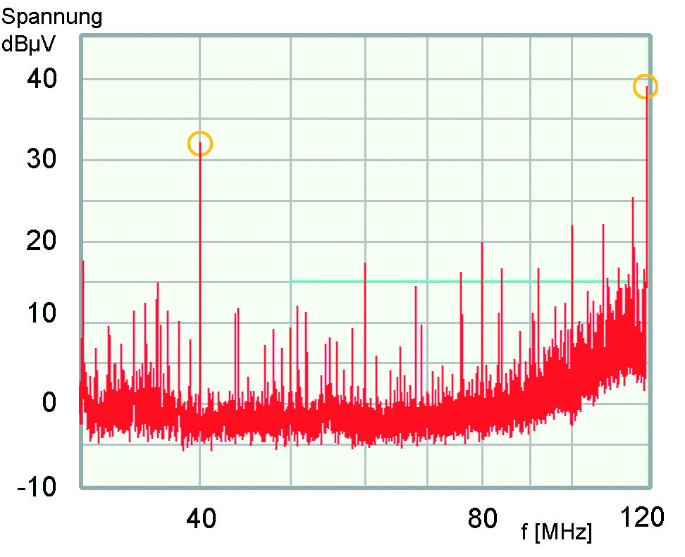
After an in-depth analysis of the board, the E-field of the installed IC was identified as the excitation source for the emission.
To interrupt this E-field coupling on the PCB assembly, a shielding part had to be designed, manufactured, and assembled above the IC. This caused additional effort and costs. If the electronics developer had understood the E-field coupling of the IC, the layout and package design of the PCB assembly could have been adapted at the IC already during the planning phase. At a later stage of development, such a measure is not always permissible. Placement changes are often no longer possible due to space limitations, component sizes, and the effort involved.
In the next step, a scan was performed with an E-near-field probe at a defined measurement distance of 20 mm above the IC. The measuring electrode of the RF-E 09 E-field probe has dimensions of 10 x 10 mm. The measurement confirms the high E-field coupling of 49 dBµV.
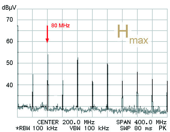
The measurement of the IC magnetic field at a distance of 20 mm showed different critical frequencies compared to the component measurement (80 MHz and 160 MHz). The maximum of the magnetic field was at 45°, and the minimum was at 135° of the IC orientation (Figure 8).
Due to fortunate circumstances, this excitation did not cause any practical problems for the board developer.
TEM Cell Measurement (IEC 61967-2)
IC manufacturers compare the fields of ICs using a TEM cell measurement. The TEM cell combines all fields of the IC into one global comparison value. The IC is placed on a 10 x 10 cm printed circuit board (TEM cell PCB) and mounted upside down in the TEM cell opening. The printed circuit board can be rotated on the opening in 90° steps (IC orientation). The IC couples into the opposite septum of the cell.
Figures 9 and 10 show a comparison measurement of two IC orientations with the TEM cell.
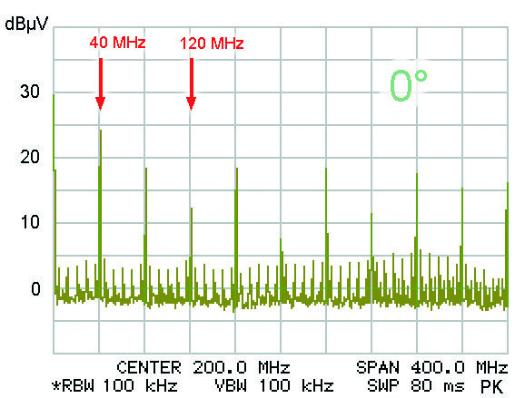
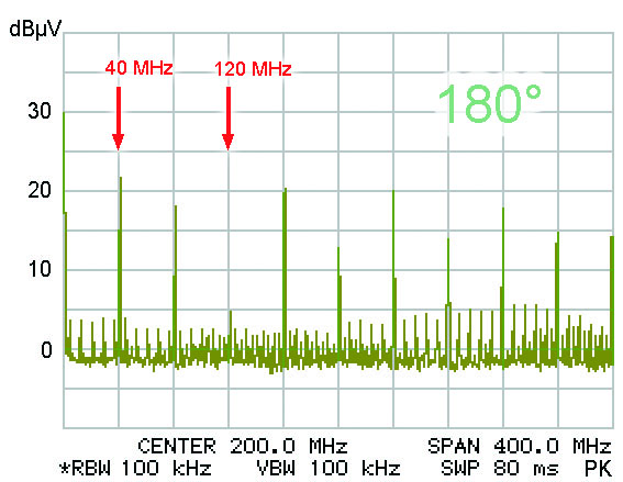
The E-field problem at 120 MHz, which is relevant in practice, is not detected here. At 120 MHz, the measured values are relatively uncritical. The highest values are measured at 40 MHz, 80 MHz, and 160 MHz. The measured value at 40 MHz was consistent with our practical example.
The TEM cell measures the electric and magnetic near field together. The electric field couples capacitively into the septum of the TEM cell, and the magnetic field couples inductively through mutual inductance. The principle corresponds to that of an E-field or H-field near-field probe. Together with the cell housing, the septum forms the induction loop of the probe.
If the IC current loop is aligned in parallel, no voltage is induced in an orthogonal orientation. The capacitive coupling is almost constant for all orientations of the loop. The coupled voltages are superimposed with their signs. Therefore, the orientations of the IC in the TEM cell produce different results. With a corresponding base orientation, a 180° rotation causes a change of sign in the induced voltage.
How the coupled voltages are composed of capacitive and inductive components depends not only on the respective coupling factors, but also on the variety of IC loops and the phase angles of the respective voltage phasors.
As determined with the previously described Surface Scan, the IC emits its maximum magnetic field in the 45° direction. In the TEM cell, however, the IC can only be rotated in full 90° steps. The TEM cell spectra show that magnetic and electric fields are superimposed.
This example shows that the results of the measurement with the TEM cell are too imprecise for our IC application. For the use of the IC on the PCB assembly, more precise information is required in order to define targeted corrective measures. As our Surface Scan with the near-field probes shows, this information is contained in the electric and magnetic near fields.
Conclusion
For EMC-compliant design of PCB assemblies, it is necessary to consider the EMC properties of ICs in advance. IC parameters should be defined, documented, and freely accessible to the developer. By considering the IC properties, the developer can better evaluate and more specifically address the increasing requirements for the design of the PCB assembly. Our example shows how important knowledge of the E-fields and H-fields of the IC can be for developers of PCB assemblies.
It is also apparent that the TEM cell cannot capture important field components. Therefore, the specific environment of the IC on the PCB assembly is also important when evaluating whether a particular IC will cause interference emissions in the application.
Consequently, an EMC-compliant design requires not only knowledge of individual IC parameters, but also their evaluation in the respective project environment.