

1 Preface
Complex devices with integrated circuits and a low supply voltage increasingly fail interference immunity tests. The localisation and elimination of weak points is a real challenge in such complex devices. The fast, specific and hence cost-saving elimination of weak points requires effective strategies and appropriate equipment for systematic immunity analysis on the board level.
2 Introduction
The reduction of the supply voltage of integrated circuits in complex modules and the associated lower noise immunity of the useful signals lead to more frequent failures in immunity tests. Standard test equipment is used to test electronic devices as a whole ("black box" principle) and hardly allows an in-depth examination of the interference current paths through the module and the identification of the actual weak points. This is the reason why filtering and shielding measures are often used in the device under test according to the trial-and-error method and are then modified until the required immunity is achieved. Lengthy searches and frequent test runs in the laboratory inevitably result in a prolonged development time, also entailing higher development costs. In addition, the manufacturing costs usually rise due to filtering and shielding that is often located in the wrong place and is thus overdesigned.
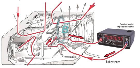
Since the test set-up for compliance testing is by no means ideal for immunity analysis, new development tools are needed to perform an immunity analysis directly in the circuit. The most important part of this toolbox is a burst generator that is designed to solve problems directly in the circuit. This burst generator continuously generates a random sequence of different voltage pulses up to an intensity of 1,500 Volt. Compared to EFT/B generators (electrical fast transient/burst) according to EN 61000-4-4, these pulses have a lower interference energy and can be injected directly into electronic modules to locate weak points. Due to direct injection, the interference energy is nevertheless sufficient to produce a similar interference effect as an externally connected EFT/B generator. The lower interference energy reduces the risk of damage to electronic components during the search for weak points. Another distinctive feature of the burst generator is its floating outputs. These floating outputs allow the developer to inject the generated pulses into selected areas of the module, even independently of the grounding system. Weak points can thus be located very quickly within a module by examining the interference current path section by section. The burst generator can also be used to supply field sources and couple the magnetic and electric fields generated by these into the module for a more detailed analysis. Furthermore, the paths on which interference current flows through a module can be analysed with magnetic field probes or an optical sensor.
The starting point for a systematic immunity analysis is a compliance test according to the standard EN 61000-4-4. The fault pattern that occurred in the compliance test provides very important information for subsequent examinations. However, the fault pattern alone does not yet allow a definite identification of the device's weak point. The display itself, for example, need not necessarily be the weak point if the display fails; the graphic controller or main processor may be responsible for the display failure instead. The fault pattern is required to simulate the module's behaviour in the compliance test for the measurement strategies described below.
3 Central Part
3.1 Analysing interference current paths
The interference current from the burst generator is led through the module via different routes to analyse the interference current paths. The analysis begins with the ground-related injection of the interference current into the module's power supply lines or interfaces and the observation of functional faults in the device under test. This approach is used to simulate the fault pattern that occurred in the compliance test. The weak point is then narrowed down in the next steps by injecting the interference current into individual sections of the module. Thanks to the burst generator's floating outputs, the interference current can also be injected into selected areas of the module independent of the grounding system.
3.2 Locating weak points with field sources
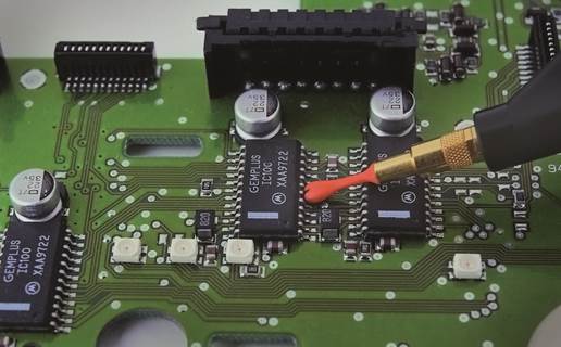
Depending on the module's packing density, weak points can be narrowed down to a certain group of components or conductor structures in most cases by analysing the interference current paths. Since the magnetic and electric pulse fields of the injected currents and voltages are mainly responsible for interference with the IC, these will be examined in the next step. These fields can be simulated with field sources and injected into selected component connections or conductor structures. Here again, the functional faults that occur in the device under test are used to narrow down the weak point. Depending on the size of the field source, the weak point can be pinpointed down to a few millimetres. Even individual sensitive IC connection pins can thus be located.
3.3 Analysing burst magnetic fields
The third measurement strategy is used to analyse the distribution of the burst magnetic fields on a module. The interference current is injected into the area to be examined on the module via conductors. The interference current generates magnetic fields around the conductors through which it flows and these can then be measured with a magnetic field probe. The magnetic field probe generates light pulses whose frequency depends on the mean magnetic flux density. The magnetic field probe is connected to the optical input of the pulse density counter that is integrated in the burst generator via an optical fibre. The value displayed on the pulse density counter is proportional to the magnetic flux density. The orientation of the magnetic field can be determined by turning and inclining the magnetic field probe. The magnetic field probe can thus be used to trace and analyse the field configuration and hence the interference current path through the module.
3.4 Monitoring logic signals and analysing immunity levels
The fourth strategy is used to monitor certain logic signals on the module by means of sensors. The sensor is connected to the signal to be monitored and converts this to light signals. Since the signals are transmitted via optical fibre, they can be measured without interaction, even under the influence of extreme interference fields. Monitoring logic signals mainly includes deterministic logic signals such as reset, clock and CE (chip enable). Data signals can also be monitored if the data sequences are known. It is important that faults can be clearly identified in the signal that is monitored. The burst generator or the field sources are used to inject the interference directly into the module. This procedure also supplies additional information about interference processes/events in the module. This is very helpful if functional faults cannot be identified from outside or are extremely delayed due to processing operations. The effectiveness of EMC measures can be checked in a similar way. A disturbed logic signal is monitored with a sensor and the values that are measured are compared with and without the implemented EMC measure. Modifications on the module can thus be assessed quickly and reliably.
4 Summary
Special measuring and testing procedures can be used to systematically inject interference pulses into individual areas of the module during development. Fault patterns are reproduced and interference current paths analysed to locate immunity weak points. The actual weak points can thus be identified quickly and efficiently. Appropriate EMC measures can be selected on this basis. The effectiveness of the measures that have been initiated is verified directly on the board. Thanks to this systematic interference immunity analysis, weak points can be identified and eliminated quickly and purposefully. This ultimately means a reduction in the development time and development costs due to fewer test runs in the laboratory and a cut in the manufacturing costs through selected and appropriate EMC measures.
5 References
- DIN Deutsches Institut für Normung e. V.: DIN EN 61000-4-4 Electromagnetic compatibility (EMC) - part 4-4. Berlin: Beuth Verlag GmbH; 2013
- Langer, G.: E1 immunity development system. Bannewitz: Langer EMV-Technik GmbH; 2014
- Langer, G.: Interference immunity – Experimental seminar, training material. Bannewitz: Ingenieurbüro Langer; 2009